

We’re trying out a new format for daily updates where we cluster news and spot directional trends instead of just adding takes on individual news items. We will have fewer but hopefully more measured takes that are focused on info density. Comment and let us know what you think.
Today, we touch up on the memory supercycle, advanced packaging buildout, and where custom silicon is going.
Let’s get into it. — Austin & Vik
Be sure to check out the Semi Doped podcast on YouTube or your favorite podcast player!
The memory supercycle is now a capital markets event
SK Hynix raised $26.5 billion in its Nasdaq debut, the largest US share sale by a foreign company, with ADRs opening at $170, 14% above the $149 offer price (Quartz). Seoul-listed shares have pulled back roughly 25% from their late-June record as investors booked profits, and the listing is widely framed as a test of the Korea discount (TradingKey). Chairman Chey Tae-won said US investment plans will far exceed the $35 billion already committed (CNBC).
The capital is chasing a supply gap that keeps widening; supply is coming online, but demand is growing even faster. To keep up, Samsung pulled the first fab at its Yongin cluster forward to 2029, one to two years earlier than planned (Korea Times).
On pricing, HBM4 is expected to roughly double from about $2 per Gb in 2H26 to $4-5 in 2027, driven by Rubin demand, long-term agreements, and HBM consuming about 3x the wafer capacity of DDR5 (digitimes, Investing.com).
Memory bandwidth is the constraint in AI compute economics, and long-term contracts are converting a cyclical business into contracted revenue.
Vik: What the memory saga has taught us all is that LLMs are useful, but its requirement for memory is a fatal flaw, not a feature. There is simply no way that people are going to blindly keep adding RAM. They. will. make. tradeoffs. It can be in terms of acceptable latency, token throughput, or model quality. A new technique that is less memory hungry will flip the world over — but it does not exist yet. Or so I think.
Austin: LLMs with significant memory/context is super useful, but blindly using expensive HBM or SRAM is the flaw imo. Hopefully this pushes for continued innovations to use cheaper flavors of DRAM and even use flash storage as a tier for KV Cache offloading, as well as algorithmic and KV cache compression improvements like sparse attention.
Packaging is where the money is landing
TSMC’s June revenue hit NT$442.68 billion, up 67.9% from June 2025, taking first-half revenue to NT$2.4 trillion, up 35.6% YoY (TSMC press release). Q2 came in around $39.6 billion, a 36% YoY rise that edged past guidance ahead of Thursday’s full report (Bloomberg).
The growth is pulling investment into packaging.
TSMC is expanding the Chiayi Science Park into a dedicated packaging hub: two Phase I plants are in or entering mass production, and Phase II broke ground this weekend with additional fabs planned (Reuters, Focus Taiwan).
Alongside the CoWoS ramp toward 200K wafers monthly in 2027, KYEC and JCET are each committing $1.4 billion to new fabs
ASE posted record Q2 revenue on AI packaging, and Liteon grew 37% YoY on AI server power (digitimes).
Supply constraints are easing, but demand is strong enough to hold pricing power for packaging and test suppliers.
Vik: Although there is a lot of capital being deployed to packaging, I’d be really interested to see where Intel’s advanced packaging revenue lands next quarter. Earnings is reported on Thursday, July 23rd, and I know I’ll be listening in. There was also some news that TSMC’s panel level packaging for large substrates won’t use glass in the initial stages. This actually makes sense to me because there is a lot of trouble in handling glass to produce high yield. There is a learning curve to scale there for the industry.
Austin: Amkor is a few days later on July 27th and is an OSAT moving into advanced packaging worth following.
Custom silicon is redrawing the foundry map
Meta’s custom inference chip Iris enters production in September, fabbed at TSMC, targeting recommendation and ranking workloads across Facebook and Instagram as part of the MTIA program (Lumien).
Samsung landed an important win. A Samsung Foundry engineer disclosed on LinkedIn that Tesla’s AI5 has completed tape-out and will be produced on Samsung’s 2nm process at Taylor, Texas (Korea Times). Tesla splits AI5 between Samsung and TSMC, with Samsung reportedly taking AI6 and TSMC handling AI6.5 (TrendForce). Running AI5 on 2nm at Taylor implies Samsung’s 2nm yields have crossed the viability threshold, and a successful ramp is the recovery path for a foundry business still in the red (Electrek).
Apple is rebuilding its Mac silicon roadmap around AI: a base M6 later this year, no M6 Pro/Max/Ultra, an AI-focused M7 family through 2027-28 with the M7 Ultra supporting up to 1.5TB of memory for Apple’s AI servers, and an M8 on a 1.4nm process in 2028 (Bloomberg).
Intel, meanwhile, announced a €5 billion ($5.7B) investment at Leixlip, Ireland, upgrading existing fabs to expand Intel 3 output for Xeon 6 and next-gen Xeon (Intel, Bloomberg). With Magdeburg cancelled last year, Leixlip is Intel’s only leading-edge site outside the US and Israel.
Austin: Meta is a Samsung story too. Meta will be ramping rack scale MTIA 400 later this year, and MI450 is supposed to be only 6 months behind that. It was recently reported by the Seoul Economic Daily that Meta is considering building MTIA with Samsung Foundry:
“Meta’s proprietary AI accelerator, the ‘MTIA,’ was produced by TSMC through its first and second generations, but the third generation unveiled this year has designated Samsung Foundry as its partner. In particular, the MTIA third generation is set to apply Samsung Foundry’s most advanced 2-nanometer process and be mass-produced on a scale of hundreds of thousands of units. A Samsung Electronics official said, “Nothing has been finalized yet.”
TSMC capacity can only grow so fast. Samsung Foundry and Intel Foundry are picking up the excess. This isn’t bearish TSMC, but it’ll be interesting to see how it impacts future TSMC expansion plans. Although it could be tempting for TSMC to increase capacity as a competitive response, I don’t think they will, and I think that’s wise. Let Samsung and Intel rise up and offtake the excess demand. The hard questions: how much should TSMC’s capacity expand and how quickly? Well, quickly enough to retain customers, satisfy as much of their growth as possible, and maintain margins.
Easier said than done.
Key Data
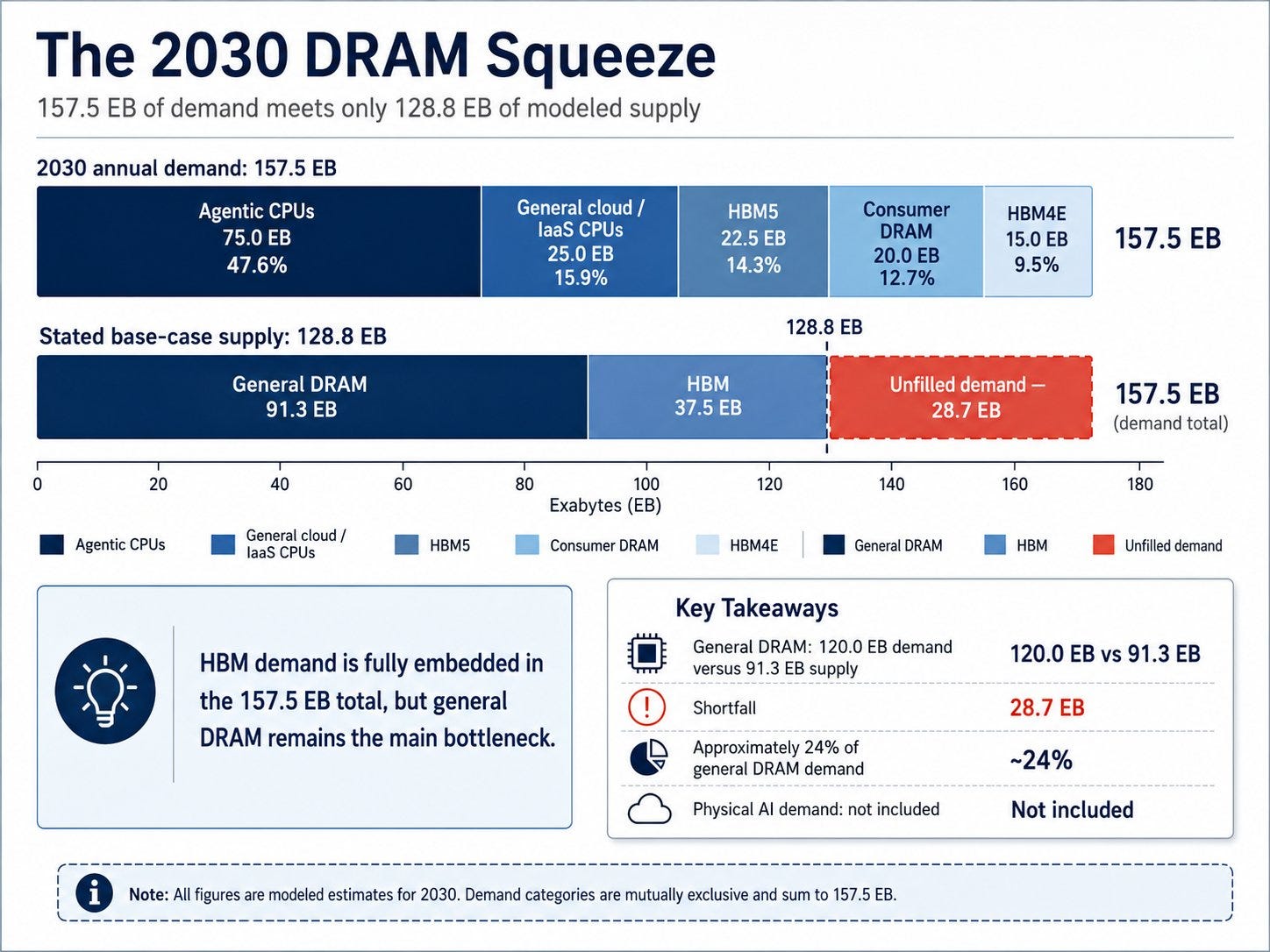
zephyr_z9 on X has an excellent article that explains how there will be a 24% shortfall in DRAM supply even in 2030. He counts the various buildouts and how much capacity they are adding, and sizes that up against expected DRAM demand.
Read the whole post.
